
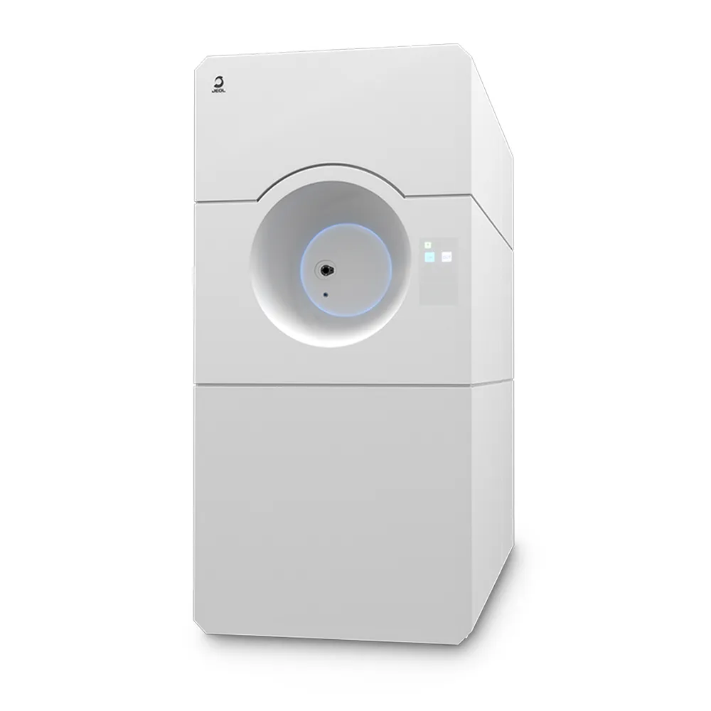
Transmission Electron Microscopy (TEM)
TEM works by passing a focused electron beam through a specimen that is typically less than 100 nanometers thick. As electrons interact with the sample, they form images or diffraction patterns that reveal fine structural, crystallographic, and compositional details. TEM is a cornerstone tool in nanotechnology, life sciences, and materials research, enabling visualization of structures far beyond the limits of light microscopy.
- Atomic to nanometer-scale resolution for internal structural analysis
- Capable of imaging morphology, crystallography, and composition
- Can be combined with analytical techniques such as EDS and EELS for elemental and chemical mapping
- Suitable for metals, polymers, semiconductors, and biological specimens
- Enables study of defects, grain boundaries, and nanostructures
- Essential for materials science, nanotechnology, and advanced biological research
- Provides diffraction analysis for crystal structure determination
Get a Quote